Your Browsing History
- In Stock
- Sold by Newegg
Quick View
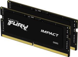
Kingston FURY Impact 64GB (2 x 32GB) 262-Pin DDR5 SO-DIMM DDR5 5600 (PC5 44800) Laptop Memory Model KF556S40IBK2-64
- CAS Latency: 40
- Timing: 40-40-40
- Voltage: 1.10V
- Multi-channel Kit: Dual Channel Kit
- Model #: KF556S40IBK2-64
- $299.99
- $271.99 –
- Save: 9%
- Free Shipping
Quick View
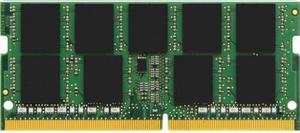
Kingston 16GB 260-Pin DDR4 SO-DIMM DDR4 2666 (PC4 21300) Memory (Notebook Memory) Model KCP426SD8/16
- CAS Latency: 19
- Timing: 19-19-19
- Voltage: 1.20V
- Model #: KCP426SD8/16
- $57.50 –
- Free Shipping
Quick View
Kingston FURY Impact 32GB (2 x 16GB) 260-pin SO-DIMM DDR4 3200 MHz CL20 Black Memory (KF432S20IBK2/32)
- CAS Latency: 20
- Voltage: 1.2 V
- Model #: KF432S20IBK2/32
- $100.99 –
- Free Shipping
Quick View
Kingston Fury Impact 8GB 260-Pin DDR4 SO-DIMM DDR4 3200 (PC4 25600) Laptop Memory Model KF432S20IB/8
- CAS Latency: 20
- Timing: 20-22-22
- Voltage: 1.20V
- Features: Power Supply: VDD = 1.2V Typical VDDQ = 1.2V Typical VPP = 2.5V Typical VDDSPD = 2.2V to 3.6V On-Die termination (ODT) 16 internal banks; 4 groups of 4 banks each Bi-Directional Differential Data Strobe 8 bit pre-fetch Burst Length (BL) switch on-the-fly BL8 or BC4(Burst Chop) Height 1.18" (30.00mm)
- Model #: KF432S20IB/8
- $49.97
- $24.99 –
- Save: 49%
- $4.99 Shipping
Quick View
Kingston FURY Impact 32GB (1 x 32GB) 260-pin SO-DIMM DDR4 3200 MHz CL20 Black Memory (KF432S20IB/32)
- CAS Latency: 20
- Timing: 20-22-22
- Voltage: 1.20V
- Recommend Use: AMD & Intel Compatible / AMD Ryzen Compatible / High Performance or Gaming Memory / Intel Compatible
- Model #: KF432S20IB/32
- $129.97
- $88.99 –
- Save: 31%
- Free Shipping

Quick View
Kingston FURY Impact 16GB (2 x 8GB) 260-Pin DDR4 SO-DIMM DDR4 3200 (PC4 25600) Laptop Memory Model KF432S20IBK2/16
- CAS Latency: 20
- Timing: 20-22-22
- Voltage: 1.20V
- Multi-channel Kit: Dual Channel Kit
- Model #: KF432S20IBK2/16
- $59.99
- $52.99 –
- Save: 11%
- Free Shipping

Quick View
Kingston FURY Impact 32GB (2 x 16GB) 262-Pin DDR5 SO-DIMM DDR5 6400 (PC5 51200) Laptop Memory Model KF564S38IBK2-32
- CAS Latency: 38
- Timing: 38-40-40
- Voltage: 1.35V
- Multi-channel Kit: Dual Channel Kit
- Model #: KF564S38IBK2-32
- $197.99
- $194.99 –
- $7.99 Shipping
Quick View
Kingston FURY Impact 32GB 262-Pin DDR5 SO-DIMM DDR5 5600 (PC5 44800) Memory (Notebook Memory)
- Part Number: KF556S40IB-32
- CAS Latency: 40
- Timing: 40-40-40
- Voltage: 1.10V
- Model #: KF556S40IB-32
- $154.97
- $135.99 –
- Save: 12%
- $7.99 Shipping
Quick View
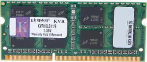
Kingston 8GB 204-Pin DDR3 SO-DIMM DDR3L 1600 (PC3L 12800) Laptop Memory Model KVR16LS11/8
- CAS Latency: 11
- Voltage: 1.35V
- Buffered/Registered: Unbuffered
- Features: JEDEC standard 1.35V (1.28V ~ 1.45V) and 1.5V (1.425V ~ 1.575V) Power Supply VDDQ = 1.35V (1.28V ~ 1.45V) and 1.5V (1.425V ~ 1.575V) 800 MHz fCK for 1600 Mb/sec/pin 8 independent internal banks Programmable CAS Latency: 11, 10, 9, 8, 7, 6 Programmable Additive Latency: 0, CL-2, or CL-1 clock 8-bit pre-fetch Burst Length: 8 (Interleave without any limit, sequential with starting address "000" only), 4 with tCCD = 4 which does not allow seamless read or write [either on the fly using A12 or MRS] Bi-directional Differential Data Strobe Internal(self) calibration: Internal self calibration through ZQ pin (RZQ: 240 ohm +/- 1%) On Die Termination using ODT pin Asynchronous Reset PCB: Height 1.18" (30mm), double sided component
- Model #: KVR16LS11/8
- $23.67 –
- Free Shipping
Quick View
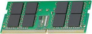
Kingston ValueRAM 32GB 260-Pin DDR4 SO-DIMM DDR4 3200 (PC4 25600) Laptop Memory Model KVR32S22D8/32
- CAS Latency: 22
- Timing: 22-22-22
- Voltage: 1.20V
- Buffered/Registered: Unbuffered
- Model #: KVR32S22D8/32
- $82.71 –
- $10.99 Shipping
Quick View
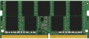
KINGSTON TECHNOLOGY KCP426SS6/4 4GB DDR4 2666MHz SODIMM
- CAS Latency: 17
- Voltage: 1.20V
- Color: Black
- Model #: KCP426SS6/4
- $26.67 –
- Free Shipping
Quick View
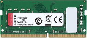
Kingston ValueRAM 8GB 2400MHz DDR4 Non-ECC CL17 SODIMM 1Rx8 (Notebook Memory) KVR24S17S8/8
- CAS Latency: 17
- Voltage: 1.20V
- Buffered/Registered: Unbuffered
- Features: Non-ECC Unbuffered 100% Factory Tested at Speed Designed to meet JEDEC Free Technical Support
- Model #: KVR24S17S8/8
- $38.33 –
- Free Shipping
Quick View
in 30 days
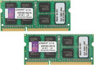
Kingston 16GB (2 x 8GB) 204-Pin DDR3 SO-DIMM DDR3 1600 Laptop Memory Model KVR16S11K2/16- CAS Latency: 11
- Voltage: 1.50V
- Multi-channel Kit: Dual Channel Kit
- Parts: Lifetime
- Model #: KVR16S11K2/16
- $59.85
- $49.50 –
- Save: 17%
- $9.99 Shipping
Quick View
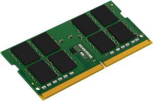
Kingston 16GB 260-Pin DDR4 SO-DIMM DDR4 3200 (PC4 25600) Laptop Memory Model KCP432SD8/16
- CAS Latency: 22
- Voltage: 1.20V
- Buffered/Registered: Unbuffered
- Model #: KCP432SD8/16
- $67.99
- $62.99 –
- Save: 7%
- $7.99 Shipping

Quick View
Kingston FURY Impact 16GB (1 x 16GB) 260-pin SO-DIMM DDR4 3200 MHz CL20 Black Memory (KF432S20IB/16)
- CAS Latency: 20
- Voltage: 1.2 V
- Model #: KF432S20IB/16
- $79.97
- $51.99 –
- Save: 34%
- Free Shipping
Quick View
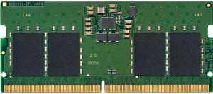
Kingston 16GB (2 x 8GB) 262-Pin DDR5 SO-DIMM DDR5 4800 (PC4 38400) Laptop Memory Model KCP548SS6K2-16
- CAS Latency: 40
- Voltage: 1.10V
- Buffered/Registered: Unbuffered
- Model #: KCP548SS6K2-16
- $90.62 –
- $10.99 Shipping
Quick View
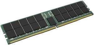
Kingston 16GB DDR5 4800MT/s ECC Reg 1Rx8 Module
- Model #: KTD-PE548S8-16G
- $147.22 –
- $10.99 Shipping
Quick View
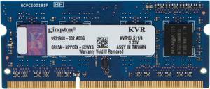
Kingston 4GB 204-Pin DDR3 SO-DIMM DDR3L 1600 (PC3L 12800) Laptop Memory Model KVR16LS11/4
- CAS Latency: 11
- Voltage: 1.35V
- Model #: KVR16LS11/4
- $18.33 –
- Free Shipping
Quick View
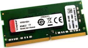
Kingston ValueRAM - DDR4 - 4 GB - SO-DIMM 260-pin - 2666 MHz / PC4-21300 - CL19 - 1.2 V - unbuffered - non-ECC
- CAS Latency: 19
- Voltage: 1.2 V
- Model #: KVR26S19S6/4
- $26.67 –
- Free Shipping
Quick View
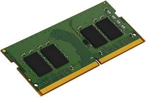
Kingston 8GB 260-Pin DDR4 SO-DIMM DDR4 3200 (PC4 25600) Memory (Notebook Memory) Model KVR32S22S6/8
- CAS Latency: 22
- Timing: 22-22-22
- Voltage: 1.20V
- Model #: KVR32S22S68
- $24.82 –
- $10.99 Shipping
Quick View
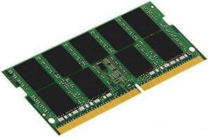
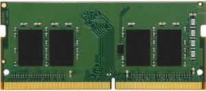
Kingston 8GB 260-Pin DDR4 SO-DIMM DDR4 2666 (PC4 21300) Memory (Notebook Memory) Model KCP426SS8/8
- CAS Latency: 19
- Timing: 19-19-19
- Voltage: 1.20V
- Model #: KCP426SS8/8
- $34.97
- $27.99 –
- Save: 19%
- $7.99 Shipping
Quick View
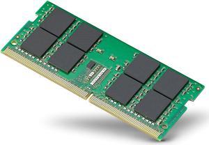
Kingston ValueRAM 4GB 260-Pin DDR4 SO-DIMM DDR4 3200 (PC4 25600) Laptop Memory Model KVR32S22S6/4
- CAS Latency: 22
- Timing: 22-22-22
- Voltage: 1.20V
- Buffered/Registered: Unbuffered
- Model #: KVR32S22S6/4
- $21.99 –
- Free Shipping
Quick View
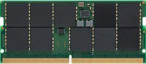
Kingston - KVR32S22D8/16 - Kingston ValueRAM 16GB DDR4 SDRAM Memory Module - 16 GB - DDR4-3200/PC4-25600 DDR4 SDRAM -
- CAS Latency: 22
- Voltage: 1.20V
- Option: 16GB
- Model #: KVR32S22D8/16
- $57.99
- $45.99 –
- Save: 20%
- $7.99 Shipping
Quick View
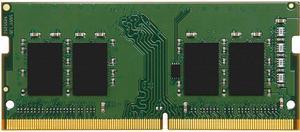
Kingston 16GB 262-Pin DDR5 SO-DIMM DDR5 4800 (PC4 38400) Memory
- CAS Latency: 40
- Voltage: 1.10V
- ECC: Yes
- Buffered/Registered: Unbuffered
- Model #: KTHPN548T16G
- $139.22 –
- $10.99 Shipping
Quick View
Kingston 8GB 260-Pin DDR4 SO-DIMM DDR4 3200 (PC4 25600) Laptop Memory Model KCP432SS6/8
- CAS Latency: 22
- Voltage: 1.20V
- Buffered/Registered: Unbuffered
- Model #: KCP432SS6/8
- $36.95 –
- Free Shipping
Quick View
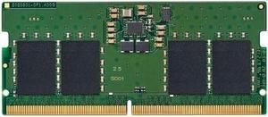
Kingston 32GB 262-Pin DDR5 SO-DIMM DDR5 4800 (PC4 38400) Laptop Memory Model KVR48S40BD8-32
- CAS Latency: 40
- Voltage: 1.10V
- Buffered/Registered: Unbuffered
- Model #: KVR48S40BD8-32
- $126.11 –
- $10.99 Shipping

Quick View
Kingston 32GB 262-Pin DDR5 SO-DIMM DDR5 4800 (PC4 38400) Memory (Notebook Memory) Model KCP548SD8-32
- CAS Latency: 40
- Timing: 40-39-39
- Voltage: 1.10V
- Part Number: KCP548SD8-32
- Model #: KCP548SD8-32
- $146.99 –
- $7.99 Shipping
Quick View
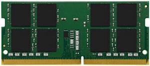
Kingston 32GB 260-Pin DDR4 SO-DIMM DDR4 3200 (PC4 25600) Memory (Desktop Memory) Model KCP432SD8/32
- CAS Latency: 22
- Voltage: 1.20V
- Option: Standard Edition
- Model #: KCP432SD832
- $106.99 –
- Free Shipping
Quick View
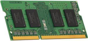
Kingston 8GB 260-Pin DDR4 SO-DIMM DDR4 2666 (PC4 21300) Laptop Memory Model KCP426SS6/8
- CAS Latency: 19
- Voltage: 1.20V
- Buffered/Registered: Unbuffered
- Model #: KCP426SS6/8
- $40.99 –
- Free Shipping

Quick View
KINGSTON 16GB DDR5 4800MT/s Module
- Model #: KCP548US8-16
- $87.99
- $79.99 –
- Save: 9%
- $7.99 Shipping
Quick View
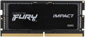
Kingston FURY Impact 16GB DDR5 SDRAM Memory Module
- CAS Latency: 38
- Timing: 38-38-38
- Voltage: 1.10V
- Buffered/Registered: Unbuffered
- Model #: KF548S38IB-16
- $82.99
- $81.99 –
- Free Shipping
Quick View
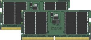
Kingston 32GB (2 x 16GB) 262-Pin DDR5 SO-DIMM DDR5 4800 (PC4 38400) Memory (Notebook Memory) Model KCP548SS8K2-32
- CAS Latency: 40
- Timing: 40-39-39
- Voltage: 1.10V
- Model #: KCP548SS8K2-32
- $134.99 –
- Free Shipping
Quick View
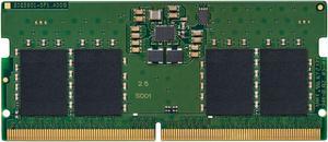
Kingston 8GB 262-Pin SODIMM DDR5 4800 CL40 SDRAM (PC5-4800) Memory Model KVR48S40BS6-8
- Model #: KVR48S40BS6-8
- $38.82 –
- $10.99 Shipping

Quick View
Kingston Impact 64GB (2 x 32GB) 260-Pin DDR4 SO-DIMM DDR4 3200 (PC4 25600) Memory (Notebook Memory) Model KF432S20IBK2/64
- CAS Latency: 20
- Timing: 20-22-22
- Voltage: 1.20V
- Multi-channel Kit: Dual Channel Kit
- Model #: KF432S20IBK2/64
- $179.22 –
- $10.99 Shipping
