Your Browsing History
- In Stock
- Sold by Newegg
Quick View
Kingston 32GB DDR5 4800MT/s ECC Reg 2Rx8 Module
- Model #: KTD-PE548D8-32G
- $267.99 –
- Free Shipping

Quick View
Kingston 64GB 5600MT/s DDR5 Non-ECC CL46 SODIMM (Kit of 2) 2Rx8
- Model #: KVR56S46BD8K2-64
- $273.99 –
- $7.99 Shipping

Quick View
Kingston 32GB 5200MT/s DDR5 CL36 DIMM FURY Beast RGB EXPO
- Model #: KF552C36BBEA-32
- $141.44 –
- $10.99 Shipping
Quick View
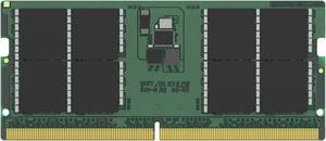
Kingston 64GB 5600MT/s DDR5 Non-ECC CL46 SODIMM (Kit of 2) 2Rx8
- Model #: KVR56S46BD8K2-64
- $269.22 –
- $10.99 Shipping

Quick View
Kingston 32GB 5200MT/s DDR5 CL36 DIMM FURY Beast Black EXPO
- Model #: KF552C36BBE-32
- $133.44 –
- $10.99 Shipping

Quick View
Kingston 32GB DDR5 4800MT/s ECC Reg 2Rx8 Module
- Model #: KTH-PL548D8-32G
- $283.22 –
- $10.99 Shipping
Quick View
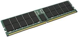
Kingston 64GB DDR5 4800MT/s ECC Reg 2Rx4 Module
- Model #: KTL-TS548D4-64G
- $532.22 –
- $10.99 Shipping
Quick View
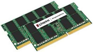
Kingston 64GB DDR5 5200MT/s SODIMM (Kit of 2)
- Model #: KCP552SD8K2-64
- $347.99
- $329.99 –
- Save: 5%
- $7.99 Shipping

Quick View
Kingston 16GB DDR5 5600MT/s Module (Kit of 2)
- Model #: KCP556US6K2-16
- $115.99
- $54.99 –
- Save: 52%
- $7.99 Shipping
Quick View
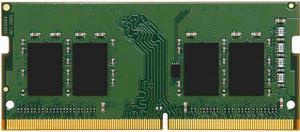
Kingston ValueRAM 8GB 260-Pin DDR4 SO-DIMM DDR4 2933 (PC4 23400) Laptop Memory Model KVR29S21S6/8
- CAS Latency: 21
- Timing: 21-21-21
- Voltage: 1.20V
- Buffered/Registered: Unbuffered
- Model #: KVR29S21S6/8
- $97.50 –
- Free Shipping

Quick View
Kingston 16GB 5200MT/s DDR5 CL36 DIMM (Kit of 2) FURY Beast RGB EXPO
- Model #: KF552C36BBEAK2-16
- $159.73 –
- Free Shipping

Quick View
Kingston 32GB 5600MT/s DDR5 CL36 DIMM (Kit of 2) FURY Beast Black
- Model #: KF556C36BBEK2-32
- $202.23 –
- Free Shipping

Quick View
Kingston 16GB DDR5 4800MT/s ECC Reg 1Rx8 Module
- Model #: KTL-TS548S8-16G
- $166.99 –
- Free Shipping

Quick View
Kingston 16GB 6400MT/s DDR5 CL38 SODIMM FURY Impact XMP
- Model #: KF564S38IB-16
- $192.25 –
- $50.00 Shipping

Quick View
KINGSTON 32GB 5600MT/s DDR5 CL40 DIMM FURY Beast Black RGB
- Model #: KF556C40BBA-32
- $258.75 –
- $50.00 Shipping

Quick View
Kingston 128GB 5200MT/s DDR5 CL40 DIMM (Kit of 4) FURY Beast RGB XMP
- Model #: KF552C40BBAK4-128
- $1,095.83 –
- $50.00 Shipping
Quick View
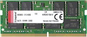
Kingston ValueRAM 16GB 2400MHz DDR4 Non-ECC CL17 SODIMM 2Rx8 (Notebook Memory) KVR24S17D8/16
- CAS Latency: 17
- Voltage: 1.20V
- Buffered/Registered: Unbuffered
- Features: Non-ECCUnbuffered100% Factory Tested at Speed Designed to meet JEDECFree Technical Support
- Model #: KVR24S17D8/16
- $52.95 –
- $9.99 Shipping
Quick View
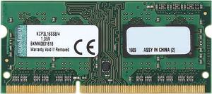
Kingston 4GB 204-Pin DDR3 SO-DIMM DDR3 1600 (PC3 12800) Laptop Memory Model KCP3L16SS8/4
- CAS Latency: 11
- Voltage: 1.35V
- Buffered/Registered: Unbuffered
- Model #: KCP3L16SS8/4
- $18.33 –
- Free Shipping
Quick View
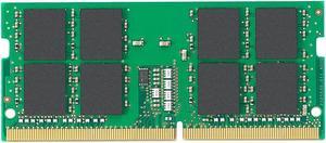
Kingston 16GB (1 x 16GB) DDR4 2400MHz DRAM (Notebook Memory) 1.2V SODIMM (260-Pin) KCP424SD8/16
- Voltage: 1.20V
- Buffered/Registered: Unbuffered
- Features: UnbufferedNon-ECC100% Factory Tested at Speed Designed to meet JEDECFree Technical Support
- Option: For iMac Retina 2017, Dell
- Model #: KCP424SD8/16
- $52.95 –
- $9.99 Shipping

Quick View
Kingston 8GB DDR4 2666 NONECC CL19 260-Pin 1.2V Memory Module KVR26S19S6/8
- CAS Latency: 19
- Voltage: 1.20V
- Timing: 19-19-19
- Color: Black
- Model #: KVR26S19S6/8
- $38.33 –
- Free Shipping
Quick View
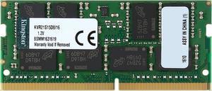
Kingston ValueRAM 16GB 260-Pin DDR4 SO-DIMM DDR4 2133 (PC4 17000) Laptop Memory Model KVR21S15D8/16
- CAS Latency: 15
- Timing: 15-15-15
- Voltage: 1.20V
- Buffered/Registered: Unbuffered
- Model #: KVR21S15D8/16
- $65.00 –
- Free Shipping
Quick View
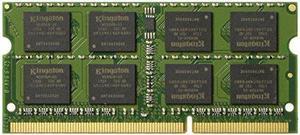
Kingston Technology 8GB 1600MHz DDR3L (PC3-12800) 1.35V Non-ECC CL11 SODIMM Intel Laptop Memory KVR16LS11/8
- CAS Latency: 11
- Model #: 8765765654545
- $23.67 –
- Free Shipping
Quick View
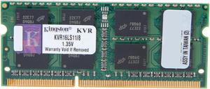
Kingston 8GB 204-Pin DDR3 SO-DIMM DDR3L 1600 (PC3L 12800) Laptop Memory Model KVR16LS11/8
- CAS Latency: 11
- Voltage: 1.35V
- Buffered/Registered: Unbuffered
- Features: JEDEC standard 1.35V (1.28V ~ 1.45V) and 1.5V (1.425V ~ 1.575V) Power SupplyVDDQ = 1.35V (1.28V ~ 1.45V) and 1.5V (1.425V ~ 1.575V)800 MHz fCK for 1600 Mb/sec/pin8 independent internal banksProgrammable CAS Latency: 11, 10, 9, 8, 7, 6Programmable Additive Latency: 0, CL-2, or CL-1 clock8-bit pre-fetchBurst Length: 8 (Interleave without any limit, sequential with starting address "000" only), 4 with tCCD = 4 which does not allow seamless read or write [either on the fly using A12 or MRS]Bi-directional Differential Data StrobeInternal(self) calibration: Internal self calibration through ZQ pin (RZQ: 240 ohm +/- 1%)On Die Termination using ODT pinAsynchronous ResetPCB: Height 1.18" (30mm), double sided component MEM_Recommend Use:
- Model #: KVR16LS11/8.
- $23.67 –
- Free Shipping

Quick View
Kingston 16GB DDR5 5200MT/s Module (Kit of 2)
- Model #: KCP552US6K2-16
- $104.99 –
- $7.99 Shipping

Quick View
Kingston 16GB 4800MHz DDR5 Non-ECC CL40 DIMM (Kit of 2) 1Rx16
- Model #: KVR48U40BS6K2-16
- $74.99 –
- $7.99 Shipping


