Your Browsing History

Quick View
Axiom 2GB DDR3 SDRAM Memory Module
- Buffered/Registered: Unbuffered
- Parts: Lifetime Limited
- Model #: MB785G/A-AX
- $237.31 –
- Free Shipping

Quick View
Kingston 16GB DDR5 4800MT/s ECC Reg 1Rx8 Module
- Model #: KTL-TS548S8-16G
- $169.99 –
- More options from $154.99 - $169.99
- Free Shipping
Quick View
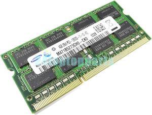
4Gb Ddr3 Pc3-12800 1600Mhz Sodimm Cl11 204Pin Chip Notebook Memory M471B5273Ch0-Ck0
- Voltage: 1.50V
- Buffered/Registered: Unbuffered
- Model #: 037-9C00DUG7AU4
- $27.99 –
- $16.99 Shipping

Quick View
VASEKY 8GB 204-Pin DDR3L SO-DIMM DDR3L 1600 (PC3L 12800) Laptop Notebook Memory
- CAS Latency: 11
- Voltage: 1.35V
- Model #: DDR3-1600-8G-NB
- $137.99 –
- $29.99 Shipping
Quick View
Dell SNP1CXP8C/16G 16GB Memory Module - DDR4 SDRAM - 3200 MHz - 260 Pin - PC-25600 - SO-DIMM - CL22 - Non-ECC Unbuffered - 1Rx8 - 1.2 Volts
- Model #: SNP1CXP8C/16G
- $233.22 –
- More options from $214.99 - $249.99
- $10.99 Shipping
Quick View
Crucial CT8G4SFD8213 8Gb Ddr4 2133 Mt/S Cl15 Drx8 Unbuffered Sodimm
- CAS Latency: 15
- Voltage: 1.20V
- Buffered/Registered: Unbuffered
- Features: Speeds start at 2133 MT/s Increase bandwidth by up to 30% Reduce power consumption by up to 40% and extend battery life Faster burst access speeds for improved sequential data throughput Optimized for next generation processors and platforms
- Model #: CT8G4SFD8213
- $39.00 –
- Free Shipping
Quick View
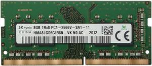
SK Hynix 8Gb 1Rx8 PC4-2666V Laptop 2666Mhz Memory SoDimm RAM HMA81GS6CJR8N-VK
- CAS Latency: 19
- Voltage: 1.20V
- Buffered/Registered: Unbuffered
- Multi-channel Kit: Dual Channel Kit
- Model #: HMA81GS6CJR8N-VKC
- $41.24 –
- Special Shipping

Quick View
SK hynix HMA851S6CJR6N - VK Non ECC PC4-2666V 4GB DDR4 at 2666MHz 260pin SDRAM SODIMM Single Kit Laptop Memory - OEM (Renewed)
- Model #: 33912923160707
- $19.91 –
- Free Shipping

Quick View
SK hynix HMA851S6CJR6N - VK Non ECC PC4-2666V 4GB DDR4 at 2666MHz 260pin SDRAM SODIMM Single Kit Laptop Memory - OEM
- Model #: 32004527226942
- $19.92 –
- Free Shipping
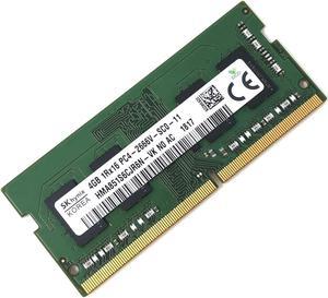
Quick View
SK hynix HMA851S6CJR6N - VK Non ECC PC4-2666V 4GB DDR4 at 2666MHz 260pin SDRAM SODIMM Single Kit Laptop Memory - OEM (Renewed)
- Model #: 32004528308286
- $19.92 –
- Free Shipping

Quick View
SK hynix HMA851S6CJR6N - VK Non ECC PC4-2666V 4GB DDR4 at 2666MHz 260pin SDRAM SODIMM Single Kit Laptop Memory - OEM
- Model #: 33912923390083
- $21.61 –
- Free Shipping

Quick View
SK hynix HMA851S6CJR6N - VK Non ECC PC4-2666V 4GB DDR4 at 2666MHz 260pin SDRAM SODIMM Single Kit Laptop Memory - OEM (Renewed)
- Model #: 32730147225703
- $22.68 –
- Free Shipping

Quick View
SK hynix HMA851S6CJR6N - VK Non ECC PC4-2666V 4GB DDR4 at 2666MHz 260pin SDRAM SODIMM Single Kit Laptop Memory - OEM
- Model #: A07GH7RRTM
- $19.92 –
- Free Shipping
Quick View
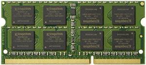
Kingston Technology 8GB 1600MHz DDR3L (PC3-12800) 1.35V Non-ECC CL11 SODIMM Intel Laptop Memory KVR16LS11/8
- CAS Latency: 11
- Model #: 8765765654545
- $23.67 –
- Free Shipping
Quick View
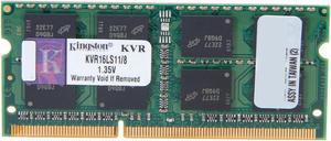
Kingston 8GB 204-Pin DDR3 SO-DIMM DDR3L 1600 (PC3L 12800) Laptop Memory Model KVR16LS11/8
- CAS Latency: 11
- Voltage: 1.35V
- Buffered/Registered: Unbuffered
- Features: JEDEC standard 1.35V (1.28V ~ 1.45V) and 1.5V (1.425V ~ 1.575V) Power SupplyVDDQ = 1.35V (1.28V ~ 1.45V) and 1.5V (1.425V ~ 1.575V)800 MHz fCK for 1600 Mb/sec/pin8 independent internal banksProgrammable CAS Latency: 11, 10, 9, 8, 7, 6Programmable Additive Latency: 0, CL-2, or CL-1 clock8-bit pre-fetchBurst Length: 8 (Interleave without any limit, sequential with starting address "000" only), 4 with tCCD = 4 which does not allow seamless read or write [either on the fly using A12 or MRS]Bi-directional Differential Data StrobeInternal(self) calibration: Internal self calibration through ZQ pin (RZQ: 240 ohm +/- 1%)On Die Termination using ODT pinAsynchronous ResetPCB: Height 1.18" (30mm), double sided component MEM_Recommend Use:
- Model #: KVR16LS11/8.
- $23.67 –
- Free Shipping
Quick View
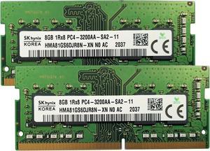
SK Hynix HMA81GS6DJR8N-XN 16GB (2X8GB) DDR4-3200MHz CP4-25600 SO-DIMM Memory Module
- CAS Latency: 22
- Voltage: 1.20V
- Buffered/Registered: Unbuffered
- Model #: HMA81GS6DJR8N-XN X2
- $70.00 –
- Free Shipping
Quick View
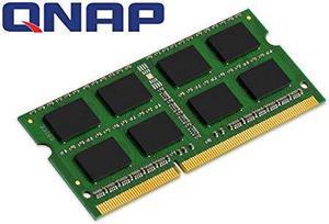
RAM-16GDR4T0-SO-2666
- Model #: RAM-16GDR4T0-SO-2666
- $414.99 –
- More options from $391.99 - $414.99
- Free Shipping
Quick View
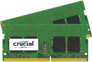
Crucial 16GB DDR4 SDRAM Memory Module
- CAS Latency: 15
- Voltage: 1.20V
- Buffered/Registered: Unbuffered
- Multi-channel Kit: Dual Channel Kit
- Model #: CT2K8G4SFS8213
- $65.00 –
- Free Shipping
Quick View
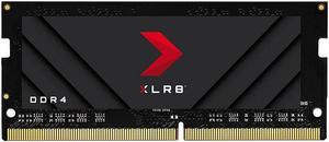
PNY 16GB XLR8 Gaming DDR4 3200MHz Notebook Memory – (MN16GSD43200X)?
- CAS Latency: 20
- Voltage: 1.20V
- Model #: MN16GSD43200X
- $90.99 –
- Free Shipping

Quick View
Crucial CT51264BC1339 4GB DDR3 SDRAM Memory Module
- CAS Latency: 9
- Voltage: 1.50V
- Buffered/Registered: Unbuffered
- Parts: Lifetime limited
- Model #: CT51264BC1339
- $18.33 –
- Free Shipping
Quick View
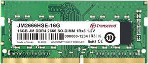
16GB Transcend JetRam DDR4 2666Mhz PC4-21300 CL19 SO-DIMM Laptop Module 260 Pins
- Voltage: 1.2V
- Model #: JM2666HSE-16G
- $111.99 –
- Free Shipping
Quick View
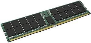
Kingston 64GB DDR5 4800MT/s ECC Reg 2Rx4 Module
- Model #: KTH-PL548D4-64G
- $529.22 –
- More options from $529.22 - $637.60
- $10.99 Shipping
Quick View
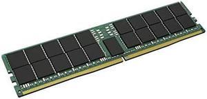
Kingston 32GB DDR5-4800MT/s ECC Module
- Model #: KTH-PL548E-32G
- $259.99 –
- More options from $259.55 - $295.30
- $7.99 Shipping

Quick View
Kingston 32GB DDR5 5200MT/s Module
- Model #: KCP552UD8-32
- $149.11 –
- More options from $149.11 - $176.33
- $10.99 Shipping

Quick View
HPE SmartMemory - DDR4 - 16 GB - DIMM 288-pin - registered 16GB DDR4 Memory Module
- Model #: 815098-B21
- $1,200.63 –
- More options from $527.99 - $1,295.99
- Free Shipping
Quick View
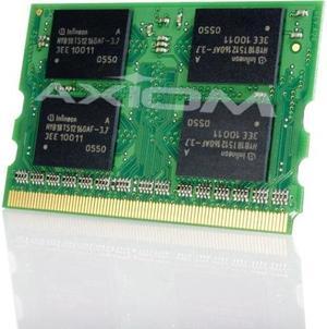
Axiom 1GB DDR 333 (PC 2700) Laptop Memory Model VGP-MM1024I-AX
- Model #: VGP-MM1024I-AX
- $700.77 –
- Free Shipping

Quick View
Axiom 4X70S69154-AX 32 GB DDR4-2666 Sodimm Memory for Lenovo
- Model #: 4X70S69154-AX
- $244.99
- $134.99 –
- Save: $110.00 (44%)
- $7.99 Shipping
Quick View
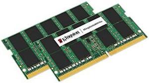
Kingston 64GB DDR5 5200MT/s SODIMM (Kit of 2)
- Model #: KCP552SD8K2-64
- $347.99
- $328.99 –
- Save: $19.00 (5%)
- $7.99 Shipping
Quick View
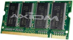
Axiom 1GB 200-Pin DDR SO-DIMM DDR 266 (PC 2100) Memory Model 311-2941-AX
OUT OF STOCK
- Buffered/Registered: Unbuffered
- Features: Dell Latitude X300
- Model #: 311-2941-AX
- $81.99 –
- $7.99 Shipping

Quick View
Axiom 1GB 200-Pin DDR SO-DIMM DDR 266 (PC 2100) Laptop Memory Model 311-3015-AX
OUT OF STOCK
- Features: Dell Inspiron Notebook: 300m 600m
- Model #: 311-3015-AX
- $82.99 –
- $7.99 Shipping

Quick View
Axiom INT2400SZ4G-AX 4GB 1.2V DDR4-2400 260-Pin SODIMM Memory Module for Intel
OUT OF STOCK
- Model #: INT2400SZ4G-AX
- $52.99
- $42.99 –
- Save: $10.00 (18%)
- $7.99 Shipping

Quick View
Axion VGP-MM512I-AX Axiom 512MB DDR SDRAM Memory Module - 512MB (1 x 512MB) - 333MHz DDR333/PC2700 - DDR SDRAM - 172-pin
OUT OF STOCK
- Model #: VGP-MM512I-AX
- $111.99 –
- $7.99 Shipping
Quick View
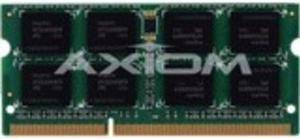
Axiom A9210967-AX Ax - Ddr4 - 8 Gb - So-Dimm 260-Pin - 2400 Mhz / Pc4-19200 - Cl17 - 1.2 V - Unbuffered - Non-Ecc - For Dell Inspiron 15, 15 3567, 15 55Xx, 17 5767, Latitude 13 33Xx, 3480, 3580, Xps
OUT OF STOCK
- Color: Black
- Model #: A9210967-AX
- $77.99
- $46.99 –
- Save: $31.00 (39%)
- $7.99 Shipping

Quick View
Axiom GX70N46761-AX Ax - Ddr4 - 4 Gb - So-Dimm 260-Pin - 2400 Mhz / Pc4-19200 - 1.2 V - Unbuffered - Non-Ecc - For Lenovo Legion Y520-15Ikbm 80Yy, Y520-15Ikbn 80Wk, Yoga 720-15Ikb 80X7
OUT OF STOCK
- Model #: GX70N46761-AX
- $47.99
- $38.99 –
- Save: $9.00 (18%)
- $7.99 Shipping
Quick View
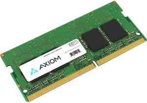
Axiom 32GB DDR4-2933 SODIMM Notebook Memory AX42933S21D/32G
OUT OF STOCK
- CAS Latency: 21
- Voltage: 1.20V
- Model #: AX42933S21D/32G
- $134.99 –
- $7.99 Shipping


